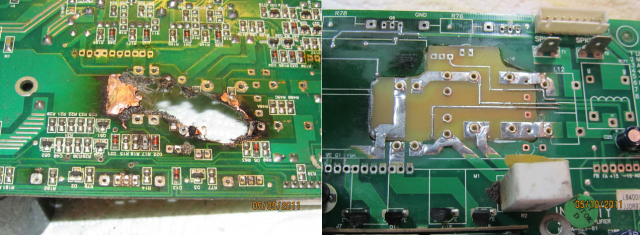
Extreme repair of PC board that was burned up after a capacitor failure. Hackaday photo.
Hackaday featured this guy’s extreme repair of his JBL subwoofer. The power board had fried — it literally burned up in a catastrophic failure caused by leaking capacitors. I looked at the details of his repair on his website and it was, quite frankly the most creative and professional repair I have ever seen. Instead of buying a new board, or ditching the subwoofer and buying a new one, he actually cut out the damaged portion of the power supply board and used the amplifier service manual and Photoshop to create a new board to fit the hole. His site is mostly pictures, the following quote is from the Hackaday article referencing his site:
[xsdb] had a real problem. His JBL L8400P 600 watt subwoofer went up in flames – literally. Four of the large capacitors on the board had bulged and leaked. The electrolyte then caused a short in the mains AC section of the board, resulting in a flare up. Thankfully the flames were contained to the amplifier board. [xsdb’s] house, possessions, and subwoofer enclosure were all safe. The amplifier board however, had seen better days. Most of us would have cut our losses and bought a new setup. Not [xsdb] he took on the most extreme PCB repair we’ve seen in a long time.
After removing the offending caps and a few other components, [xsdb] got a good look at the damage. the PCB was burned through. Charred PCB is conductive, so anything black had to be cut out. The result was a rather large hole in the middle of an otherwise serviceable board. [xsdb] had the service manual for the JBL sub. Amazingly, the manual included a board layout with traces. Some careful Photoshop work resulted in an image of the section of PCB to be repaired. [Xsdb] used this image to etch a small patch board.
The amplifier and patch were milled and sanded to match up nearly perfectly. Incredibly, all the traces aligned. [Xdsb] soldered the traces across the join with small sections of wire and solder wick. After soldering in some new high quality capacitors, the amplifier was back in action!
(published from Fort Wayne, Indiana)